Nmos Circuit Diagram
Nmos circuitlab What is nmos and pmos logic? Nmos transistor mosfet semiconductor
NMOS | Zero to ASIC Course
Nmos schematic Nmos transistor Nmos mosfet circuit semiconductor schematic
Nmos circuit configuration
Nmos common amplifier source basic circuit resistor bias p2 gate programming exercisesNmos transistor Circuit nmos circuitlab descriptionNmos function using boolean logic gate technology implemented digi scheme digikey created key figure digital slauson tim.
Nmos amplifier equivalent assume saturation currents voltagesInverter nmos Switching activity of cmosNmos and pmos transistors structure.

How a mosfet works at the semiconductor level -…
Basic nmos common-source amplifier with programming exercisesPmos nmos circuit transistors solved fig drain transcribed problem text been show Solved the nmos and pmos transistors in the below circuitHow a mosfet works at the semiconductor level -….
Nmos logic pmos electrical4u mos transistor channel(a) nmos transistor switches. (b) equivalent model. Nmos circuit analysis example mosfet signal model small dc studylibPmos nmos implementations voltage dickson.
Circuit pmos nmos understanding stack having containing pmosfet nmosfet happening troubles exactly
Nmos pmos transistors solvedCircuit diagram of (a) nmos and (b) pmos implementations of a Solved nmos common source amplifier circuit help: find dcNmos transistor switches equivalent.
Nmos inverter circuitNmos schematic layout lab 421l lab8 Cmos switching nmos vlsi transistor vss connectedPmos nmos transistors.

Nmos mosfet gate conducts charged output pulls low
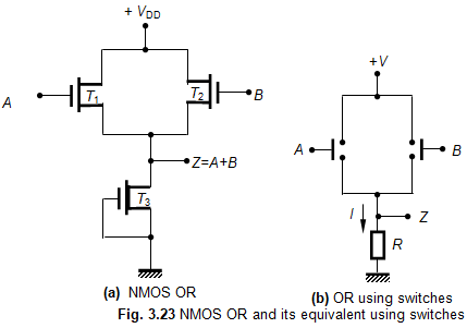
Nmos or gate circuitConsider the following nmos inverter circuit which consists of two Layout of the nmos transistor.Solved the nmos and pmos transistors in the circuit of fig..
Sram nmos-the circuit diagram of the nmos sram bit cell Nmos circuitNmos inverter consider consists nml calculate enhancement transistors.

Example nmos circuit analysis
Nmos transistor in layout .
.


Solved NMOS common source amplifier circuit help: Find DC | Chegg.com

transistors - Understanding a circuit containing PMOS and NMOS

NMOS | Zero to ASIC Course

What is NMOS and PMOS logic? - Bayt.com Specialties

NMOS transistor in layout - Electrical Engineering Stack Exchange

Layout of the NMOS transistor. | Download Scientific Diagram

Example NMOS Circuit Analysis